Note: this article was originally written in Portuguese for one the magazines where the author contributed and them translated to English to be part of one of its books.
Opening any piece of electronic equipment, the reader will find that the electronic components are mounted on a special board of fiber or another insulating material.
This support or chassis for the components is called a printed circuit board (PCB).
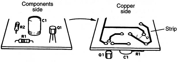
The board, as shown in Figure 1, is made of an insulating material where copper strips are printed on one or both sides.

The strips act as wires, conducting the currents from one component to another.
The pattern of the strips is determined by the function of the circuit.
All the strips are planned before the manufacturing process to provide the necessary connections between components in the desired function.
This means that a printed circuit board produced to receive components that form a radio can’t be used to mount TV circuits or any other equipment.
As shown in Figure 2, the small components are soldered onto the board so their terminals make contact with the copper strips.
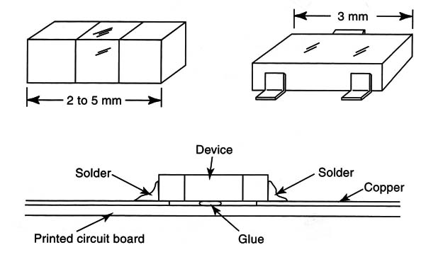
In some cases, when the components are very small as in surfacemounted devices (SMD), they can be placed on the board at the same side of the strips as shown in Figure 3.
Removing and reinstalling components on a printed circuit board is a delicate operation that an electrician who wants to work with electronics, to repair and mount circuits, must know.
Special techniques are required for this work because the components are so small and extremely sensitive to heat.
The solder used in electronics is an alloy formed of 60 percent tin and 40 percent lead with some rosin.
It is common to call this kind of solder transistor solder, radio-TV solder, or 60-40 solder.
When heated to about 273 degrees Celsius, the solder melts and involves the terminal of the component which fixes it to the board, while at the same time providing electric contact with the copper strips or other components.
When working on component mounting or replacement, an electrician will need some solder and a soldering iron.
The solder can be bought in small quantities as shown in Figure 4.

A soldering iron is shown in Figure 5.
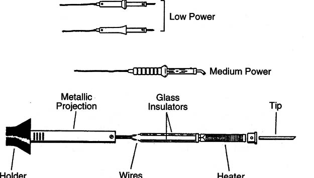
A 25 to 40-watt soldering iron with a shiny tip is recommended when working with small electronic components found in circuits.
Of course, the reader can also have a heavy-duty soldering iron to remove or place larger components like those found in some electric and electronic applications.
Radio Shack has soldering irons suitable for this task as well as the next task:
Dual Wattage Pencil Iron, 15 to 30 W (Radio Shack 64-2060)
15 W Pencil (Radio Shack 64-2052)
25 W Pencil (Radio Shack 64-2072)
Soldering is a simple operation and many readers are familiar with this kind of work.
But, electronic devices are very special and care should be taken when soldering to avoid damaging them.
Many electronic devices are easily damaged by excess heat or the incorrect soldering procedure.
The basic procedures to solder electronic components (remove or install on a PCB) are as follows:
Plug in the soldering iron and heat for at least five minutes. This is long enough to bring the tip to the correct temperature for good soldering operation.
Touch the soldering iron to the work area, allow a very short time for the connection to heat up, and then touch the solder to the connection, not the iron, as shown in Figure 6.
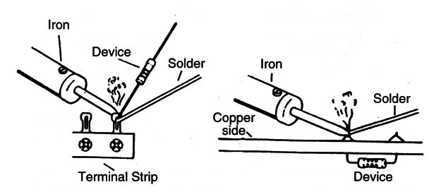
You will notice that when the solder melts it penetrates every part of the solder joint.
Remove the iron and do not move the joint until it has had time to cool. It is easy to see when the joint is cool. A peculiar haze will pass over the hot metal after which, the joint is cool enough and strong enough to withstand movement.
Figure 7 shows a perfect solder joint and some solder joints with problems.
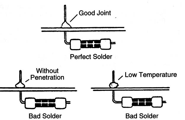
One of the principal causes of problems in electronic equipment is “cool solder.”
The solder seems to involve the component, but no electric contact is established because the joint was not heated enough to penetrate the metal creating an isolated layer of moisture or oxide to form between them.
Although the use of the soldering gun, such as the one shown in Figure 8, is not forbidden, there are many cases in electronic works in which it is not recommended.
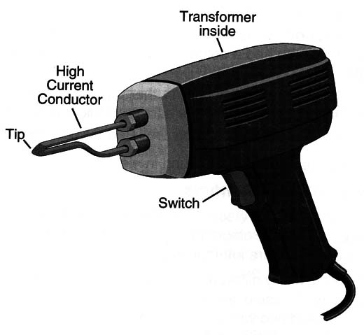
This type of soldering tool has its resistive tip heated by a strong cur rent coming from the low-voltage winding of a transformer.
When working with sensitive components such as integrated circuits, transistors, and others during the soldering operation, this current can be enough to burn them.
Today is a tendncy to not use lead in any application, as it is toxic and can be release to ambient with nocive effects.
So, the reader can find appliances where lead-less solder is used.
This solder have a higher fusion point needing special irons to work with it.
