

The way the transistor are biased and how the signals to be amplified or controlled are applied ad taken off a circuit determine three basic configurations shown by figure 1.
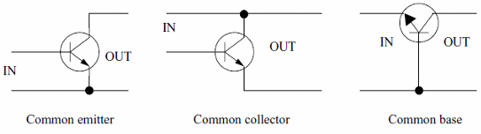
General Characteristics of Transistor Circuits
| Common Emitter | Common Base | Common Collector |
| Large voltage gain | Large voltage gain | Near unity voltage gain |
| Large current gain | Near unity current gain | Large current gain |
| Highest power gain | Medium power gain | Lowest power gain |
| Low input resistance | Very low input resistance | High input resistance |
| High output resistance | Very high output resistance | Low output resistance |
Figure 2 shows how a transistor is used in the two basic operation modes (linear and saturated). In (a) the load is placed between the power supply and the collector of a NPN transistor. The resistor in the base determines the amount of base current. This resistor is named "biasing resistor". When closing S1 the base current cause the current to flow through the load.
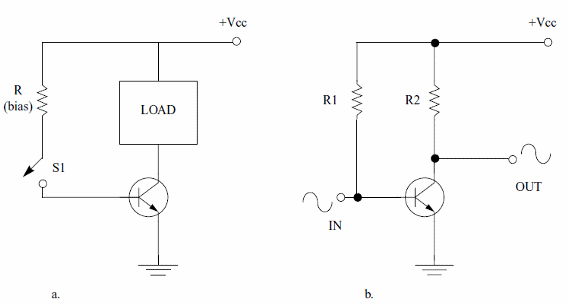
If, as shown in (b) a variable current, as the correspondent to an audio signal, is applied to the base the small variations if this current will produce large variations in the collector current.
The way the transistor are biased and how the signals to be amplified can be applied and taked off a circuit determines three basic configurations of the transistors.
The three ways or basic configurations are shown in figure 3.
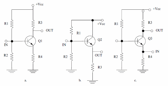
In (a) we have the common emitter configuration presenting larger voltage and current gain (power gain). In (b) we have the common emitter configuration giving a high current gain but low voltage gain and in (c) the common base configuration.
According the aplication one configuration can have best performance than other and is preferred.
Normally, more than one transistor is used in any application. Each transistor is the center of a stage and the amplified signals must pass from one to other stage, being amplificated until reach the desired level.
The basic applications of Power transistor in Mechatronics is as control for high current loads as shown by figure 4.
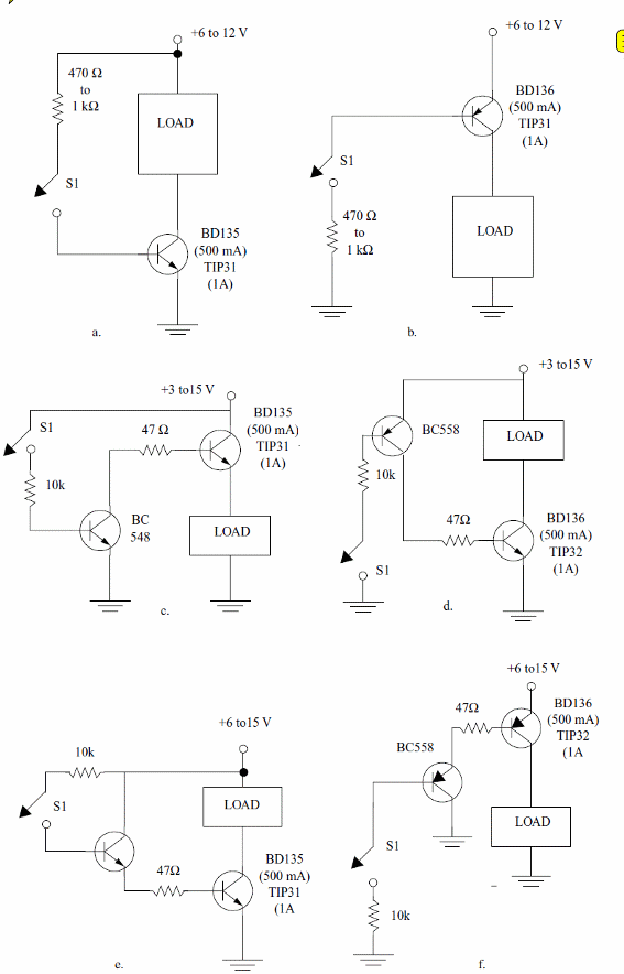
The resistor R is dimensioned to source to the base current enough to cause the current needed by the load, considering the gain of the transistor.
The configurations are:
a) Common NPN
b) Common PNP
c) Complementary I
d) Complementary II
e) Darlington NPN
f) Darlington PNP
Formula:
An approximate formula to determine the resistor R is the next:
R = [ (Vcc – 0.6) / Ic ] * β
Where:
R is the value of the resistor (Ω)
Vcc is the power supply voltage (V)
Ic is the collector or load current (Ic)
β is the gain of the transistor
a) The value calculated is the maximum to saturate the transistor. For practical purposes use a value 20% to 30% lower than the calculated.
b) Use the minimum β (gain) of the considered transistor.


