

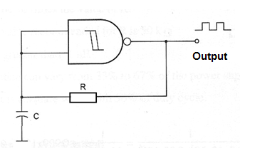
The basic configuration of a 4093 wired as astable multivibrator is shown in figure bellow. The time the output on is the interval in which the capacitor charges to the trigger point (T1) and the time the out[put is low is the interval the capacitor needs to discharges to the holding point (T2). As T1 is different from T2 the output is a square wave with duty cycle different from 50%.
The next formulas are valid to calculations involving this circuit:
Formula 1
Periods:
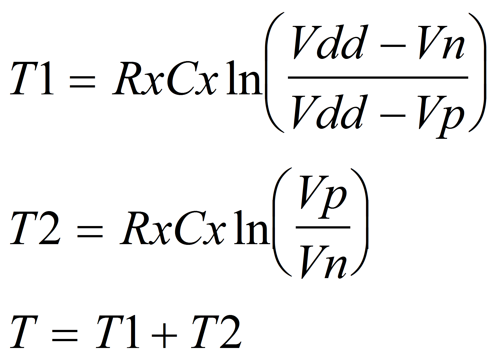
T is the total period in seconds (s)
T1 is the period to the output in the high level in seconds (s)
T2 is the period to the output in the low level in seconds (s)
R is the resistance in ohm (Ω)
C is the capacitance in farads (F)
Vdd is the power supply voltage in volts (V)
Vp is the positive threshold voltage in volts (V)
Vn is the negative threshold voltage in volts (V)
TABLE - Threshold Voltages of the 4093 CMOS IC
Next table shows the values of threshold voltages as function of the power suply voltage applied to the 4093 IC.
| Characteristic | Vdd | Value |
| Positive Threshold Voltage (Vp) | 5 10 15 |
1.8 4.1 6.3 |
| Negative Threshold Voltage (Vn) | 5 10 15 |
3.3 6.2 9.0 |
Note: the values in the table are typical for the 4093B IC from National Semiconductor. Small variations can be noted according the manufacturer. It is important to note that these characteristics also change with the temperatuie.
Formula 2
Frequency:
f = 1 / T
f = 1 / (T1 + T2)
Where:
f is the frequency in hertz (Hz)
T is the total period given by formula 124.1 in seconds (s)
T1 and T2 are the periods calculated by formula 124.1 in seconds (s)


