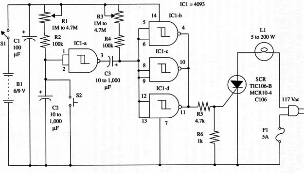
The circuit works as follows. When S1 is closed, capacitor C2 charges through R1 and R2 until Vp is reached. At this moment, the IC 1-a output goes to a low logic level, and C3 begins to charge through R3 and R4 until VI1 is reached.
During the first capacitor charge (C2), IC1-b, c, and d outputs remain at the low level, and the SCR is off. During the second time delay, when C3 is charging, ICl-b, c, and d outputs remain high, and the SCR is triggered on, supplying the lamp from the ac power line.
As soon as the capacitor C3 is charged to Vn, ICl-b, c, and d outputs go to a low logic level again, and this causes the SCR to trigger off. To set a new time delay, you have to discharge C2 by pressing S2.
Remember that the SCR is a half-wave control to ac loads. A diode bridge can be used to give you a full-wave control. Do not use inductive loads or fluorescent lamps in this circuit.
A schematic diagram for the Incandescent Lamp Dual Timer is shown in Fig. 1.

The positions of the polarized components [power supply (dc) and electrolytic capacitors must be correct. The SCR must be mounted on a heatsink.
With a 1,000 µF capacitor for C2 and C3, and 4,700,000 ohm potentiometers, the total time delay is up to 90 minutes. Current drain from the dc power supply is very low, extending battery life to several weeks.
IC1 - 4093 CMOS integrated circuit
SCR - TIC106-B or equivalent silicon thyristor
S1 - SPST toggle or slide switch
S2 - SPST momentary switch, normally open
R1, R3 - 1,000,000 ohm to 4,700,000 ohm potentiometers
R2, R4 - 100,000 ohm, 1/4 W, 5% resistors
R5 - 4,700 ohm, 1/4 W, 5% resistor
R6 - 1,000 ohm, 1/4 W, 5% resistor
C1 - 100 µF, 12 WVDC electrolytic capacitor
C2 - 10 µF to 1,000 µF, 12 WVDC electrolytic capacitor
F1- 5 A fuse and holder
B1 - 6 V or 9 V (four AA cells or battery)


