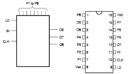
Description: This package contains a Parallel-In/Serial-Out Shift Register that can be used as a B, 7, or 8 stage shift-right register either as a serial in/serial out or as a parallel in/serial out circuit.

Pin Names
Vdd - Positive Supply Voltage
Vss - Ground
Q6, Q7, Q8 - Outputs
P1, PE, P3, P4, P5, P8, P7, P8 - Parallel Inputs
CLK - Clock
IN - Data Input
LD – Load

Operation Mode:
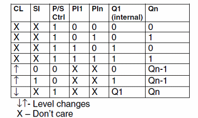
a) Serial-In/SeriaI-Out Operation:
* The LD input is grounded.
* Data applied in the IN input is shifted to the first stage on the positive transition of the clock pulse.
* After six successive clock cycles data appears at the output pin Q6.
º In the next clock pulse, the data goes to the output Q7, and yet another to the output Q8.
* Additional clock pulses lose the data or recirculate it if stages are cascaded.
b) Parallel-In/SeriaI-Dut Operation:
* An 8-bit word is loaded through the parallel inputs Pi to P8. (P1 near the input and P8 near the output)
* When LD goes to the “1” logic level, data is loaded into the register.
* After this operation, LD must be returned to ground.
The pulses applied to the clock shift the data loaded into the register to the right.

Other Devices:
A similar device with synchronous load is the 4014.
Applications:
Registers
Data Conversion
Observations:
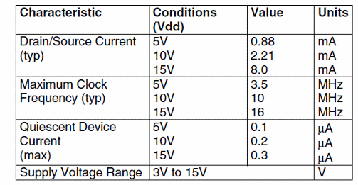
Fast clock transitions are needed to avoid incorrect operation of the device.


