

Description: This package contains a full Divide-by-B Counter. This device is synchronous and produces a square wave as output.

Pin Names:
Vdd - Positive Supply Voltage
Vss - Ground
Q0, Q1, Q2, Q3, Q4, Q5, Q8, Q7 - Outputs
CLK - Clock or Input
EN - Enable
RST - Reset
C/OUT - Output [see operation mode]
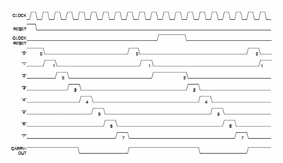
Timing Diagram: Instead of the truth table, a timing diagram is given for this device.
Operation Mode:
EN and RST must be grounded.
Any positive transition of the clock makes the circuit advance one count
The decoded output goes to the “1” logic level [positive] and the others remain at the “0" state [ground].
The OUT output remains in the “1 " level for counting from 0 to 8 and goes to the “0” logic level when counting from 4 through 7.
Reset is completed by putting the RST terminal to the “1 " logic level. RST must be back to the “0” to allow the count to continue.
A “1 ” applied to the EN input inhibits the clock operation and stops the count.

Other Devices:
The 4017 is a similar counter, but presents 10 outputs. With appropriate connections it can be used to count up to 8 like this device.
Applications:
Counters
Frequency Dividers
Timers
Observations:
External gates can be used to make divisions from 1 to 8.


