
- This device is formed by a circuit that converts Binary-Coded-Decimal into a 1-of-10 output. The same device can be used to convert a 8-bit code into a 1-of-8 output.
-
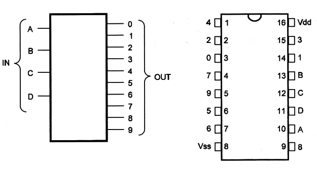
- Functional Diagram or/and Package:
-
-
-
-
Pin Names:
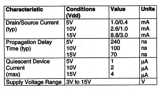
Vdd - Positive Supply Voltage (3V to 15V)
-
Vss - Ground
-
A, B, C, D - BCD Inputs
- 0, 1, 2, 3, 4, 5, 6, 7, 8, 9 - Decimal Outputs
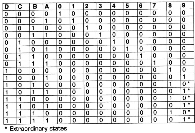
- Truth Table
-
-
Operation Mode:
-
a) BCD to 1-of-10
- BCD codes are applied to the A, B, C, and D inputs. The least significant bit is applied to A and the most significant to D.
- The output that goes to the “'1” logic level depends on the input (see the truth table).
- An invalid state depends on the origin of the chip (manufacturer).
-
b) 1-of-8 decoder
- The input D is grounded.
- The logic signals to be decoded are applied to inputs A, B, and C.
- The output depends on the logic levels applied to the input (see the truth table).
- Electrical Characteristics
-
-
-
-
Applications:
-
Code Conversion
-
Address Deooding - Memory Controls
-
Driver for Displays (tubes)
-
-
Observations:
-
Outputs can be relabeled for other codes.
-
-
4028 BCD to Decimal Decoder (CM025E)
- Details
- Written by: Newton C. Braga


