

Functional Diagram and/or Package:
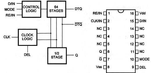
Pin Names:
Vdd - Positive Supply Voltage [SV to 'lSV]
Vss - Ground
RE/IN - Recirculate Input
CLK/ IN - Clock Input
O - Data Output
O/ - Complementary Data Output
O/ IN - Data ln
MODE - Mode Control
DEL - Delayed Clock Output
Truth Table
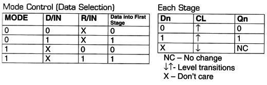
Operation Mode:
a) MODE Input Grounded - mode 1
- MODE is grounded.
- Data to be stored is applied to the Data-ln terminal [D/IN). Data enters the circuit at the positive transition of the clock signal.
- After 64 clock pulses, data applied to the input appears at pin ES and the complement at pin 7.
b) MODE Input at “'1” logic level - mode 2
- MODE input is at “”1” logic level.
- Data is applied to the RE/IN Input and stored in the circuit with the positive transition of the clock signal.
- For recirculation, REC IN is connected to OUT.
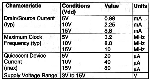
Electrical Characteristics:
Applications:
-
Shift Registers [serial]
-
Time Delay Applications
-
-
Observations:
-
The terminal OUT can be used as an input to a following register.
-
This allows for cascading stages in multiples of 64.
-
The outputs can drive one TTL input.
-
The clock input has a high input capaoitanoe of about 60 pF.


