

-
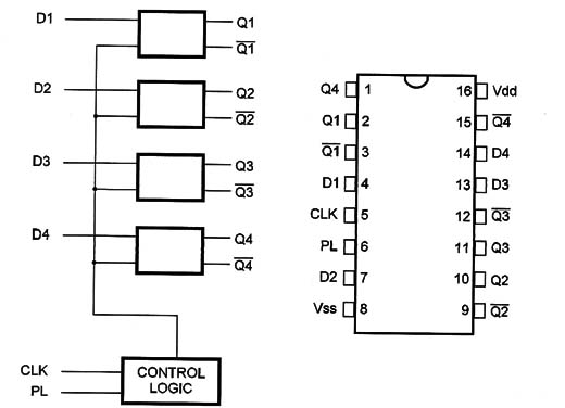
Description: This device is formed by four D-type latches with level-controlled storage command pins.
-
-
Functional Diagram and/or Package:
-
-
-
-
Pin Names:
-
Vdd - Positive Supply Voltage [BV to 15V]
-
Vss - Ground
-
D1, D2, D3, D4 - D Inputs
-
Q1, Q2, Q3, Q4 - Outputs
-
Q1/, Q2/, Q3/, Q4/ - Complementary Outputs
-
CLK - Clock
-
PL – Polarity
-
-
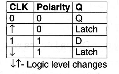
Truth Table:
-
-
-
Operation Mode:
-
With PL=0 and ST=0, data applied to D appears in the outputs [Q and (Q/).
-
Passing PL to “1' data in the input is stored at the negative transition of the clock pulse.
-
The output follows one state of the Store Control.
-
-
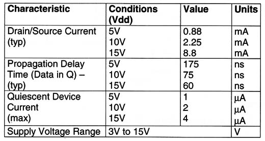
Electrical Characteristics:
-
-
-
-
Applications:
-
Buffer Storage ' Digital Logic ' Holding Registers
-
-
Observations:
-
Stages using this device may not be cascaded.


