

Description: This device is formed by six independent inverters. It is a general-purpose device intended for applications Where high noise immunity is required.
Functional Diagram and/or Package:
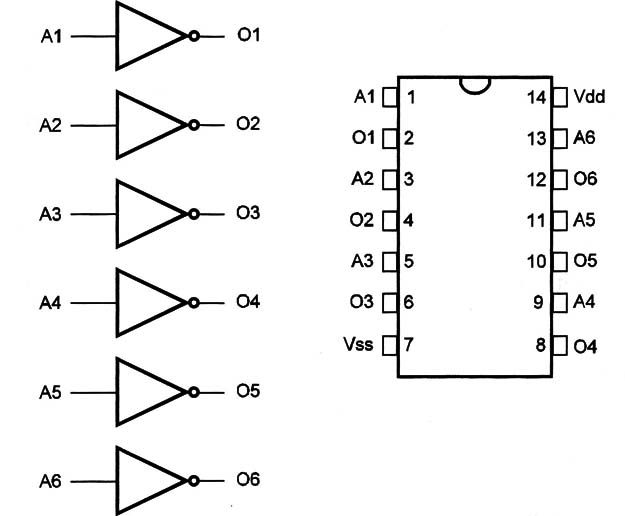
Pin Names:
Vdd - Positive Supply Voltage [BV to 15V]
Vss - Ground
A1, A2, A3, A4, A5, A6 - Inputs
O1, O2, O3, O4, O5, O6 – Outputs
Truth Table:
| A | O |
| 0 | 1 |
| 1 | 0 |
Operation Mode:
The logic signals applied to the input of each inverter appear inverted in the output [see Truth Table].
Electrical Characteristics:
Other Devices:
If you need more output current, the 4049 is recommended.
Applications:
Inversion of Logic
Oscillators
Pulse Conditioning
Digital Amplifiers [high impedance]
Observations:
This circuit can drive two low-power TTL inputs or one TTL LS input.


