

Description: This device is formed by four D flip-flops with common clock, disable, clear input, and tri-state outputs.
Functional Diagram or/ and Package:
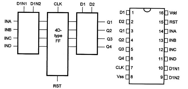
Pin Names:
Vdd - Positive Supply Voltage [3V to 15V]
Vss - Ground
INA, INB, INC, IND - Inputs
Q1, Q2, Q3, Q34 - Dutputs
CLK - Clock
RST - Reset
D1, D2 - Disable output
DIN1, DIN2 - Disable input
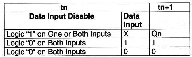
Truth Table:
Operation Mode:
Pins 1, 2, 9, 10, and 15 are grounded for normal operation.
Data applied to the D inputs is stored in the circuit With the positive transition of the clock pulse.
If pins 9 and 10 are “'1” [DlN1 and DIN2], data applied to the input will be ignored.
If pins 1 and 2 are “1” (D1, D2], the outputs go to the tri-state condition.
Reset is done by placing pin 15 to the “1” logic level.
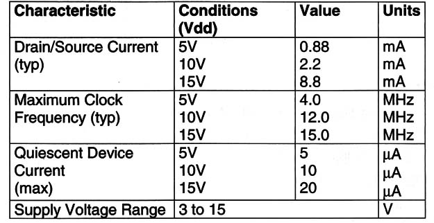
Electrical Characteristics:
Applications:
Interfacing
Data Storage


