

Description:
This device is a 5-stage divide-by-10 Johnson Counter with ID decoded outputs and a carry out bit. The decoded output goes to the “’1" logic level remaining the others in the “0” logic level.
Functional Diagram and/ or Package:
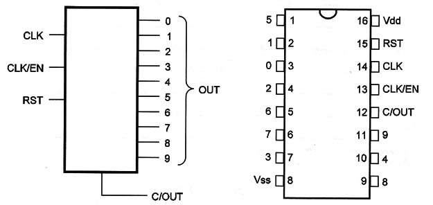
Pin Names:
Vdd - Positive Supply Voltage [3V to 15V]
Vss - Ground
OUT0 to OUT9 - Decoded Outputs
RST - Reset
CLK - Clock or Signal Input
CLK EN - Clock Enable
C/OUT - Carry Out Output
Timing diagrams:
Instead of the truth table, the operation of the 4017 can be clarified by looking at the timing diagram shown in Figure 1.

Operation Mode:
In the normal operation RST and CLK EN are kept at the ground [0] and the pulses are applied to the CLK input.
The circuit advances one count on the positive going transition of the clock pulse or signal.
Reset is done by putting a “1” at the RST input.
Each decoded output remains at the “1” logic level during the full clock cycle. The other remains at the “0” logic level.
The carryout pulse is produced at the final of the full counting.
The 4017 can be programmed to count up to values lower than 10 [2 and 9]. To count up to N, simply connect the output n+1 to the RSTas shown in Figure 2.
")
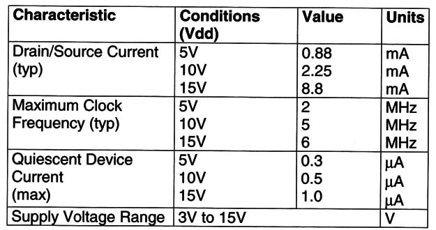
Electrical Characteristics:
Applications:
Decade Counters [sequencer]
Binary Counter with Decoder
Frequency Dividers
Timers
Divide-by-N Counters


