

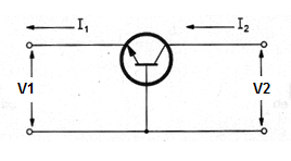
Figure bellow shows the common base configuration using a NPN transistor with the main parameters to be used in the next formulas. In this configuration the signal to be amplified is applied to the emitter and is taken from collector. The base is the common element to the input and output signals as it is wired to the ground.
Formulas 1
Common base:
V1 = Vbe
I 1 = Ie
V2 = Vbc
Where:
Vbe is the voltage between base and emitter in volts (V)
Ie is the current flowing through the emitter in amperes (A)
Vbc is the voltage between base and collector in volts (V)
Ic is the current flowing through the collector in amperes (A)


