

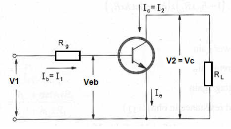
When used in the common emitter configuration the transistor is wired as shown in figure. RL is the load resistance and Rg is the generator resistance.
Note: to make easier the use of the next formulas the index "e" used to indicate that the hybrid parameters are expressed to this configuration were suppressed. So, instead write h21e we are using only h21.
Formula 1
Current amplification:
GI = Ic / Ib
GI = h21 / (1 + h22 x RL)
Where
GI is the current gain
The other parameters are defined in table (MA096).
Formula 2
Voltage gain:
Gv = Vec / Veb
Gv = (h21 x RL) / (h11 x det h x RL)
Where :
Gv is the voltage gain
Other parameters are defined in table (MA096).
Formula 3
Input resistance:
Rin = Veb / Ie
Rin = (h11 + det h x RL) / (1 + h22 x RL)
Where
Rin is the input resistance in ohm (Ω)
Other parameters are defined in table (MA096).
Formula 4
Output resistance:
Rout = Iec / Ic
Rout = (h11 + Rg) / (det h + h22 x Rg)
Where:
Rout is the output resistance in ohm (Ω)
Other parameters defined as in table (MA096).
Formula 5
Power gain:
Gp = (h212) / [ (1 + h22 + RL) x (h11 + det h x RL) ]
Where
Gp is the power gain
The other quantities are defined as in table (MA096).
Formula 6
Power gain with impedance matching:
Gp = ( 4 x Rg x RL x h212 ) / [Rg(1 + h22 x RL) + (h11 + det h x RL ]2
Where
Gp is the power gain
Other parameters are defined in table (MA096).


