

Translated into English by Patricia Lima Carlos
This article is from 1989, based on an operational amplifier of the time. However, the settings can be used on more modern operations.
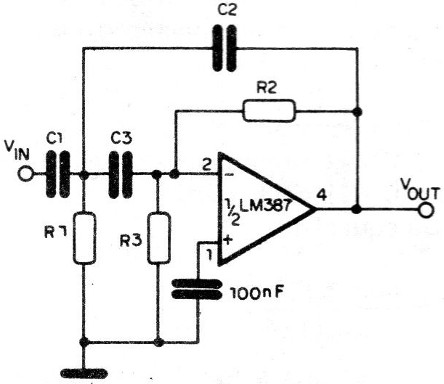
A type of high-pass filter (which lets only pass frequencies above a certain value) is shown in Figure 1 and is based on half an LM387 double operational.
To better understand how to use this integrated circuit, it will be interesting to see, firstly, how we can use it in the amplifier function, and from there we will move to the design of filters.
LM387
LM387 consists of a double amplifier, supplied in an 8-pin DlL package, as shown in Fig. 2.
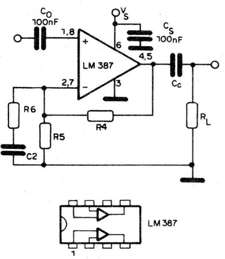
In the same figure, we also have the configuration normally used for this integrated as non-inverter pre-amplifier for AC signals.
The values of the components follow the following relations:
R4 = (
Vs
2,6
- 1 ) R5
R5 = 240 k (máx)
AVAC = T +
R4
R6
(R5 > R6)
C2 = 1/2 π fo R6
Cc = 1/2 π f RL
fo = lower frequency limit (-3dB) (f <fo)
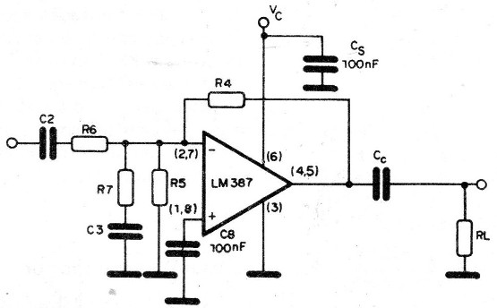
For high level signals, greater than 300 mV, the inverter configuration is more appropriate. Voltage gains of less than 20 dB are possible in this configuration, since the R5 resistor acts as a voltage divider for the input signals. In Figure 3, we have the circuit proposed by National.

In order to have a unit gain, it is necessary to take into account the stability, the gain of the amplifier between pins 2 and 4 (7 and 5 in the other channel) is at least 10, in all operating frequencies.
The gain is given by the relationship between the feedback resistor R4 and the total net impedance seen in relation to the inverting input.
This calculation neglects the impedance of the signal source.
In the diagram of Figure 4, the net impedance seen from the inverting input is given by R 5 // R6 at high frequencies. At low frequencies, where the feedback gain is high, the impedance of the inverting input is low and R5 is not effectively present in the circuit.
At high frequencies, the gain of the feedback loop decreases, which causes the input impedance to increase to the limit set by R5.
At these frequencies, R5 acts as a divider for the input voltage, guaranteeing for the amplifier a gain equals to 10, when properly chosen. If the ratio of R4 divided by R5 // R6 is at least 10, the stability of the circuit will be assured.
As long as R4 is typically 10 times R5 (for high supply voltages) and R6 equals R4 (for unit gain), the circuit will be stable without the need for additional components.
For low voltage applications where the R4 to R5 ratio is less than 10, it is necessary to connect a series RC circuit in parallel with R5 in such a way that the high frequency ratio satisfies the design requirements for the set gain.
The equations for this circuit are: IAvl (between pins 2 and 4)
R4
R5 // R6 // R7
≥ 10
RY = R5 // R6
R7 ≤
RY x R4
10 ( RY – R4 )
An example of application for these formulas is given in the National Semiconductor Audio / Radio Handbook: designing a unit gain amplifier and low noise level to operate with a voltage supply Vs: 12V with lower frequency limit of 20 Hz, impedance of input of 20 k and 100 k load impedance.
Solution
1. Rin = R6 = 20k.
2. For unit gain we must make R4 = R6, that is, R4 = 20 k.
3. From the circuit of Figure 3, we calculate the relation between R4 and R5 for the desired conditions:
R4 = (
Vs
2,6
) RS = (
12
2,6
- 1 ) R5
R4 = 3,62 x R%
From this relation, we calculate R5:
R5 =
R4
3,62
R5 =
20 k
3,62
R5 = 5.525 k
We use the closest commercial value: RS = 5k6
4. From the equation RY = R5 // R6 (RS in parallel with R6) we have:
RY =
5k6 x 20k
5k6 + 20k
Ry = 4,375
5. From the equation:
R7 ≤
RY x R4
10RY – R4
We Have:
R7 =
4,375 x 20 x 103
10 x 4,375 - (20 x 103)
R7 = 3,684 - we used for R7 3k6.
6. For fo = 20Hz, we have:
C2 = 1/2 π fo R6 = 1 / (2π x 20 x 20k)
R7 = 3.98 x 10 π
We used C2 = 0.5 uF (or 0.47 uF)
For a cut at f = 20 Hz with -3dB, the calculations must predict a factor 4 times lower at least, i.e., f
We then:
Cc =
1
2 π R L
Cc =
1
2 π x 5 x 100 k
Cc = 3,18 x 10⁻⁷
We can use the nearest commercial value, which is 330 nF.
7. The selection of C3 is arbitrary, since its effect occurs only at high frequencies. A proposed frequency for the calculation is the upper limit of the band, i.e., 20 kHz.
We then:
C3 = 1 / ( 2π x 20 k x R7 )
C3 = 1 / (2π x 20 k x 3,6 k)
C3 = 2,21 x 10⁻⁹
The nearest commercial value used will be 2n2.
HIGH-PASS FILTERS
For the filter in Figure 4, the polarization elements are calculated exactly as in the previous item, in the case of R2 and R3. Once these components are fixed, it will be enough to choose the bandwidth, gain and factor Q to calculate the other components, according to the following formulas:
Calculated by the expression:
ωo = 2πfc
Q factor:
ωc = ωo / β
η = √ [ 1 – (1 / 202)2 + 1 ]
β = √ [ 1 – (1 / 202) + η ]
Making C1 = C3
C1 =
Q
10
(2 Ao + 1)
C2 =
C1
Ao
R1 =
1
Qωo C1 (2Ao + 1)
Here's an example project. Design a bipolar active filter to be used with a rumble filter.
Its characteristics should be: gain (Ao) = 1; Q = 0.707 (Butterwort) and lower cutoff frequency fc = 50 Hz.
The supply voltage is Vs = + 24 V.
Solution
1. Set R3 to 240k.
R3 = 240k
2. From the initial part we calculate R2:
R2 = (
Vs
2,6
- 1 ) R3 = (
24
2,6
- 1 )
240 k = 1,98 x 10⁶
we used, in practice, 2 M.
3. For Q = 0.707 we have:
ωo = ωc = 2 π fc
4. Set C1 = C3.
5. Eq.
Q
ωo R2
(2Ao / 1)
5. From the equation:
C1 =
Q
ωo R2
C1 =
0,707 x (2 + 1)
2π x 50 x (2 x 106)
C1 = 3,38 x 10⁻⁹
We use a capacitor of 3n3, which is the closest commercial value. C3 will be equals to C1. So:
C1 = C3 = 3n3
6 - Equation
C2 =
C1
Ao
C2 =
C1
1
C1 = 3n3
R1 =
1
Qωo [ 1 ( Ao + 1 ) ]
R1 =
1
0,707 x 2π x 50 x (0,0033 x 10-6) x (2 + 1)
R1 = 45,5 x 10⁴ ohms
We use the nearest commercial value, which is 470 k.
R1 = 470k
In Figure 5, we have the final diagram with all the calculated values.
Through the equation we can check several characteristics of the project, and, therefore, it is very useful. The capacitor C4, of 10 nF, is placed in the circuit to ensure stability in the projects of unit gain.
LOW-PASS FILTER
In Figure 6, we have the diagram of a filter which lets signals pass only of frequencies below a certain value. The design involves inverse rationale for the high-pass filter, since the polarization resistor R4 will be calculated last.
Knowing Ao, Q and fc, first, we calculate the constant K, by the equation:
arbitrarily, we select C1 to have a convenient value. From there we have:
K =
1
4Q2 x (Ao + 1)
C2 = K x C1
The equations already seen allow us to calculate wo from wc. From there we take:
R2 =
1
2Qωo x C1 x K
R3 =
R2
Ao + 1
R1 =
R2
Ao
R4 =
R2 + R3
[ (Vs / 2,6) – 1 ]
The National Semiconductor manual also provides an excellent example of calculation. Designing an active two-pole low-pass filter to be used as a scratch filter. Its characteristics: gain (A0) = 1, Q = 0.707 (Butterworth) and lower cut-off frequency fc = 10 kHz. The supply voltage is Vs = + 24 V.
From the equations we have:
1. First, the value of K:
1
4 x 0,7072 x (1 + 1)
K = 0,25
2. We select C1 = 560 pF (arbitrary choice).
3. The calculation of C2 is done below.
C2 = K C1 = (0.25) (560 p) = 140 pF
We use a capacitor of 150 pF for C2.
4. Starting from Q = 0.707, (wo =: wc = 2 x 3.14 x fc, we continue.
5. We then calculate R2:
R2
1
2 x 0,707 x 2π x 10k x 560p x 0,25
we used an 82k resistor.
6. We then calculate R3:
R3 =
82k
2
R3 = 41k
we use R3 = 39k
7. From the equations already seen, we calculate R4:
R4
82k + 39k
[ (24 / 2,6) – 1 ]
R4 = 14,7 k
The standard value used is 15 k.
The complete filter diagram is shown in Figure 7.

The capacitor C3 is added along with the input lock capacitor C4 to give stability to the circuit. The following equation helps in checking the values ??and verifying the stability.
CONCLUSION
These are just some of the possible applications for this type of component, having its characteristics as high-pass and low-pass filters. We can also obtain combined connections which result in bandpass filters, which can be used in tone controls and even in equalizers.


